- 您现在的位置:买卖IC网 > Sheet目录484 > NIF9N05CLT1 (ON Semiconductor)MOSFET N-CH 52V 2.6A SOT223
�� �
�
�NIF9N05CL,� NIF9N05ACL�
�Protected� Power� MOSFET�
�2.6� A,� 52� V,� N� ?� Channel,� Logic� Level,�
�Clamped� MOSFET� w/� ESD� Protection�
�in� a� SOT� ?� 223� Package�
�http://onsemi.com�
�Benefits�
�?� High� Energy� Capability� for� Inductive� Loads�
�?� Low� Switching� Noise� Generation�
�V� DSS�
�(Clamped)�
�52� V�
�R� DS(ON)� TYP�
�107� m� W�
�I� D� MAX�
�2.6� A�
�Features�
�?�
�?�
�?�
�?�
�?�
�?�
�Diode� Clamp� Between� Gate� and� Source�
�ESD� Protection� ?� HBM� 5000� V�
�Active� Over� ?� Voltage� Gate� to� Drain� Clamp�
�Scalable� to� Lower� or� Higher� R� DS(on)�
�Internal� Series� Gate� Resistance�
�Pb� ?� Free� Packages� are� Available�
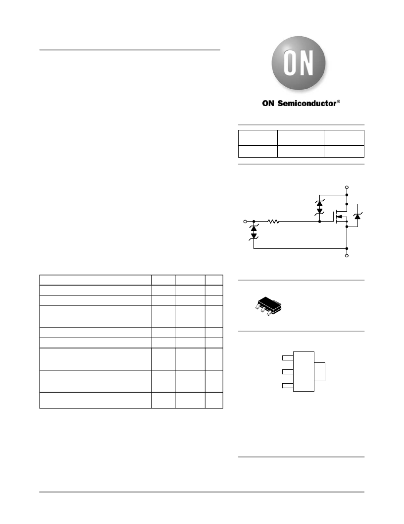
�Gate�
�(Pin� 1)�
�R� G�
�Overvoltage�
�Protection�
�Drain�
�(Pins� 2,� 4)�
�M� PWR�
�Applications�
�?� Automotive� and� Industrial� Markets:�
�Solenoid� Drivers,� Lamp� Drivers,� Small� Motor� Drivers�
�MAXIMUM� RATINGS� (T� J� =� 25� °� C� unless� otherwise� noted)�
�ESD� Protection�
�Source�
�(Pin� 3)�
�Rating�
�Drain� ?� to� ?� Source� Voltage� Internally� Clamped�
�Symbol�
�V� DSS�
�Value�
�52� ?� 59�
�Unit�
�V�
�Gate� ?� to� ?� Source� Voltage� ?� Continuous�
�Drain� Current�
�?� Continuous� @� T� A� =� 25� °� C�
�?� Single� Pulse� (t� p� =� 10� m� s)� (Note� 1)�
�Total� Power� Dissipation� @� T� A� =� 25� °� C� (Note� 1)�
�Operating� and� Storage� Temperature� Range�
�V� GS�
�I� D�
�I� DM�
�P� D�
�T� J� ,� T� stg�
�±� 15�
�2.6�
�10�
�1.69�
�?� 55� to� 150�
�V�
�A�
�W�
�°� C�
�SOT� ?� 223�
�CASE� 318E�
�STYLE� 3�
�MARKING� DIAGRAM�
�Single� Pulse� Drain� ?� to� ?� Source�
�Avalanche� Energy� (V� DD� =� 50� V,� I� D(pk)� =� 1.17�
�A,� V� GS� =� 10� V,� L� =� 160� mH,� R� G� =� 25� W� )�
�Thermal� Resistance,�
�Junction� ?� to� ?� Ambient� (Note� 1)�
�Junction� ?� to� ?� Ambient� (Note� 2)�
�E� AS�
�R� q� JA�
�R� q� JA�
�110�
�74�
�169�
�mJ�
�°� C/W�
�GATE�
�DRAIN�
�SOURCE�
�1�
�2�
�3�
�4�
�DRAIN�
�Maximum� Lead� Temperature� for� Soldering�
�Purposes,� 1/8� ″� from� Case� for� 10� Seconds�
�T� L�
�260�
�°� C�
�(Top� View)�
�Stresses� exceeding� Maximum� Ratings� may� damage� the� device.� Maximum�
�Ratings� are� stress� ratings� only.� Functional� operation� above� the� Recommended�
�Operating� Conditions� is� not� implied.� Extended� exposure� to� stresses� above� the�
�Recommended� Operating� Conditions� may� affect� device� reliability.�
�1.� When� surface� mounted� to� a� FR4� board� using� 1� ″� pad� size,� (Cu� area� 1.127� in� 2� ).�
�2.� When� surface� mounted� to� a� FR4� board� using� minimum� recommended� pad�
�size,� (Cu� area� 0.412� in� 2� ).�
�A� =� Assembly� Location�
�Y� =� Year�
�W� =� Work� Week�
�xxxxx� =� F9N05� or� 9N05A�
�G� =� Pb� ?� Free� Package�
�(Note:� Microdot� may� be� in� either� location)�
�ORDERING� INFORMATION�
�See� detailed� ordering� and� shipping� information� in� the� package�
�dimensions� section� on� page� 5� of� this� data� sheet.�
�?� Semiconductor� Components� Industries,� LLC,� 2011�
�November,� 2011� ?� Rev.� 6�
�1�
�Publication� Order� Number:�
�NIF9N05CL/D�
�发布紧急采购,3分钟左右您将得到回复。
相关PDF资料
NILMS4501NR2G
IC MOSF N-CH 9.5A 24V ESD 4-PLLP
NJ28RA0104F--
THERMISTOR NTC 100KOHM 1%
NL276C2G
INDICATOR 105-130V GREEN
NL589C2A
LAMP NEON PNL MNT 125V AMBER
NL589WL2G
LAMP NEON PNL MNT 125V GREEN
NMSD200B01-7
MOSFET N-CH 60V 200MA SOT363
NOA1302DCRG
AMBIENT LIGHT SENSOR SSPO8
NOIH2SM1000S-HHC
IC SPACE IMAGE SENSOR 84-JLCC
相关代理商/技术参数
NIF9N05CLT1G
功能描述:MOSFET 52V 2.6A N-Channel RoHS:否 制造商:STMicroelectronics 晶体管极性:N-Channel 汲极/源极击穿电压:650 V 闸/源击穿电压:25 V 漏极连续电流:130 A 电阻汲极/源极 RDS(导通):0.014 Ohms 配置:Single 最大工作温度: 安装风格:Through Hole 封装 / 箱体:Max247 封装:Tube
NIF9N05CLT3
功能描述:MOSFET 52V 2.6A N-Channel RoHS:否 制造商:STMicroelectronics 晶体管极性:N-Channel 汲极/源极击穿电压:650 V 闸/源击穿电压:25 V 漏极连续电流:130 A 电阻汲极/源极 RDS(导通):0.014 Ohms 配置:Single 最大工作温度: 安装风格:Through Hole 封装 / 箱体:Max247 封装:Tube
NIF9N05CLT3G
功能描述:MOSFET 52V 2.6A N-Channel RoHS:否 制造商:STMicroelectronics 晶体管极性:N-Channel 汲极/源极击穿电压:650 V 闸/源击穿电压:25 V 漏极连续电流:130 A 电阻汲极/源极 RDS(导通):0.014 Ohms 配置:Single 最大工作温度: 安装风格:Through Hole 封装 / 箱体:Max247 封装:Tube
NIFP-1601
制造商:NI 制造商全称:National Instruments Corporation 功能描述:Analog Input Modules for Compact FieldPoint and FieldPoint
NIFP-AI-100
制造商:NI 制造商全称:National Instruments Corporation 功能描述:Analog Input Modules for Compact FieldPoint and FieldPoint
NIFP-AI-102
制造商:NI 制造商全称:National Instruments Corporation 功能描述:Analog Input Modules for Compact FieldPoint and FieldPoint
NIFP-AI-110
制造商:NI 制造商全称:National Instruments Corporation 功能描述:Analog Input Modules for Compact FieldPoint and FieldPoint
NIFP-AI-111
制造商:NI 制造商全称:National Instruments Corporation 功能描述:Analog Input Modules for Compact FieldPoint and FieldPoint